

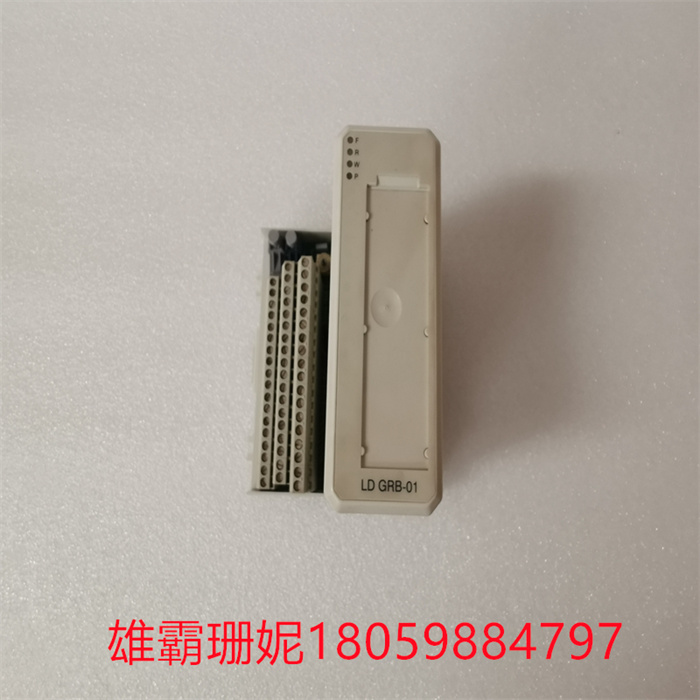
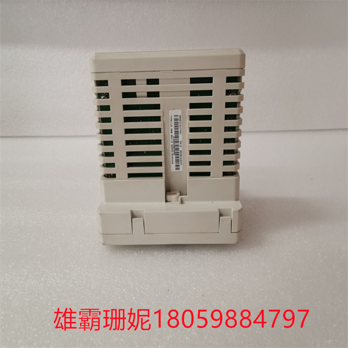
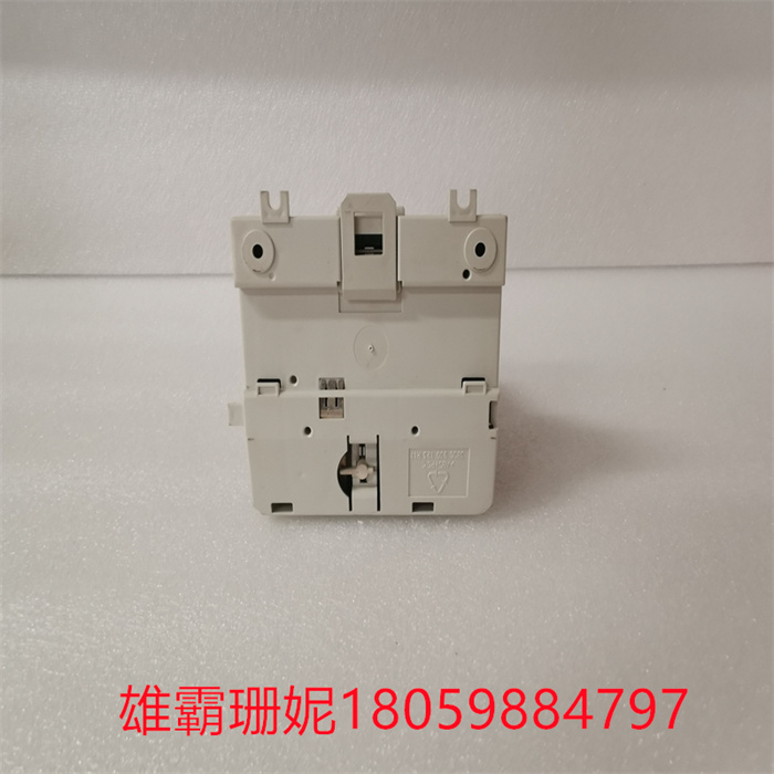
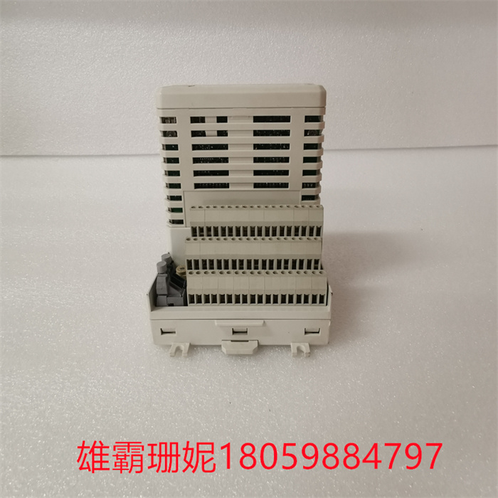
ABB LDGRB-01 3BSE013177R1 PLC自动化备件
品牌
功率
批号
特色服务
电源电压
电源电流
处理器速度
数量
可售卖地
用途
类型
型号
ABB LDGRB-01 3BSE013177R1 PLC自动化备件
MB86S02视频图像传感器在FPGA的控制下进行视频图像信息的采集,在收到PC机的采集命令后MB86S02开始视频信号的采集 FPGA作为系统的核心控制单元不仅负责视频图像的采集,而且负责视频图像信息的预处理和系统各单元模块之间的数据交互。针对视频图像数据量大的特点,为了保证系统的实时性要求,系统采用大容量的片外SDRAMR对采集到的视频图像信息进行缓存,SDRAM控制器由FPGA实现,视频图像信息经过 SDRAM缓存后首先要由FPGA对其进行滤波处理,以消除图像信息中的噪声干扰,本系统中采用中值滤波的方式对采集到的视频信息进行处理,滤波后的数据通过FPGA内部FIFO进入DSP进行下一步的压缩处理。DSP上电后首先进行引导程序的自加载,等待FPGA发送请求,在收到FPGA的请求后,DSP建立EDMA通道从FPGA获取视频数据,存满一帧后,开始对视频图像进行JPEG压缩处理,压缩处理后的视频图像信息经过FIFO缓存后,在 FPGA的控制下写入USB接口控制器的数据缓存区,等待PC机的读数请求,USB接口控制器在收到PC机的读数请求后将数据写入PDIUSBD12的端口1,以便PC机下一步读取数据。
2系统软件总体设计
系统的软件设计根据硬件结构的总体划分,也可以分为两大部分来描述。整个系统的运行如图2所示,FPGA和DSP各自的程序独立运行,通过中断信号完成数据的实时交互。FPGA向DSP方向的指令是通过FPGA发送一个EDMA请求,DSP通过响应EDMA请求,建立EDMA通道,开始从FIFO中进行预处理后数据的读取,DSP向FPGA传输数据时,通过向FPGA发送一个中断信号,让其从FIFO中把压缩后的图像数据读出来。
整个系统工作流程可以简单描述如下:系统上电后,首先DSP由flash实现自举,并运行引导程序,之后转入EDMA等待状态,FPGA初始化后等待外部图像采集命令,收到图像采集命令后开始进行图像采集,并对采集到的图像进行预处理,预处理后的图像经过FIFO缓冲,在存储一定量的数据之后,FPGA通过半满信号向DSP发送EDMA请求,等待DSP响应,DSP一旦收到来自FPGA的EDMA请求,立即建立EDMA通道,从FIFO中读取数据到L2存储器,存满一帧图像后DSP开始图像压缩,等待一幅图像压缩完成之后,DSP会向FPGA发送中断信号,FPGA在收到中断信号后开始从 FIFO中读取压缩后的图像数据。一帧数据读完后,判断编码信号是否有效,如果有效则按同样的规则对下一帧图像进行压缩,如果无效则通知DSP结束。
3结论
本设计方案已经经过了硬件验证,达到了预定的设计要求,实现了大数据量的实时处理。
系统体积仅为70×70mm,功耗小于5W,中值滤波速率平均20F/S,JPEG压缩速率平均25F/s以上。不仅满足了视频处理系统的实时性要求,且体积小、功耗低,而且基于FPGA的可编程性,本系统具有良好的灵活性和扩展性。
ABB LDGRB-01 3BSE013177R1 PLC自动化备件
MB86S02 video image sensor collects video image information under the control of FPGA. After receiving the acquisition command from PC, MB86S02 starts to collect video signals. As the core control unit of the system, FPGA is not only responsible for the collection of video images, but also for the preprocessing of video image information and the data interaction among all units and modules of the system. In view of the large amount of video image data, in order to ensure the real-time requirements of the system, the system uses a large-capacity off-chip SDRAMMR to cache the collected video image information, and the SDRAM controller is realized by FPGA. After the video image information is cached by SDRAM, it must be filtered by FPGA to eliminate the noise interference in the image information. In this system, the collected video information is processed by median filtering, and the filtered data enters the DSP through the internal FIFO of FPGA for further compression. After the DSP is powered on, it first loads the boot program and waits for the FPGA to send a request. After receiving the request from the FPGA, the DSP establishes an EDMA channel to obtain video data from the FPGA, and after storing a full frame, it starts JPEG compression of the video image. After the compressed video image information is buffered by the FIFO, it is written into the data buffer area of the USB interface controller under the control of the FPGA, waiting for the reading request of the PC. The USB interface controller writes the data into port 1 of PDIUSBD12 after receiving the reading request from the PC, so that the PC can read the data next.
2 overall design of system software
According to the overall division of hardware structure, the software design of the system can also be described in two parts. The operation of the whole system is shown in Figure 2. The programs of FPGA and DSP run independently, and the real-time interaction of data is completed through interrupt signals. The instruction from FPGA to DSP is to send an EDMA request through FPGA. DSP responds to the EDMA request, establishes an EDMA channel, and starts to read the preprocessed data from FIFO. When DSP transmits data to FPGA, it sends an interrupt signal to let it read the compressed image data from FIFO.
The workflow of the whole system can be simply described as follows: after the system is powered on, first, the DSP is bootstrapped by flash, and the boot program is run, and then it turns to the EDMA waiting state. After the FPGA is initialized, it waits for the external image acquisition command, and after receiving the image acquisition command, it starts to acquire the image, and preprocesses the acquired image. The preprocessed image is buffered by FIFO, and after storing a certain amount of data, The FPGA sends an EDMA request to the DSP through a half-full signal, waiting for the DSP to respond. Once the DSP receives the EDMA request from the FPGA, it immediately establishes an EDMA channel, reads data from the FIFO into the L2 memory, and starts image compression after a frame of image is filled. After an image compression is completed, the DSP sends an interrupt signal to the FPGA, and the FPGA starts reading the compressed image data from the FIFO after receiving the interrupt signal. After reading a frame of data, it is judged whether the coded signal is valid. If it is valid, the next frame of image is compressed according to the same rules. If it is invalid, it is notified to DSP to end.
3 Conclusion
This design scheme has been verified by hardware, achieved the predetermined design requirements, and realized the real-time processing of large data.
The volume of the system is only 70×70mm, the power consumption is less than 5W, the average median filtering rate is 20F/S, and the average JPEG compression rate is above 25 F/s.. It not only meets the real-time requirements of video processing system, but also has small volume and low power consumption. Based on the programmability of FPGA, this system has good flexibility and expansibility.